
VL812 4端口USB 3.0集散控制器是第三代全集成的单芯片解决方案,强调低功耗设计和行业首个集成的5V DC-DC开关稳压器。VL812提供高性能,高功率效率,并减少了整体系统BOM,使其成为移动和其他低功耗应用的理想选择。
VIA实验室的VL812集线器控制器支持更高的USB 3.0规范的传输速率,允许高达5Gbps的最大数据传输速率,或10倍的吞吐量可用的USB 2.0。除了快速传输,VL812集成了电池充电控制器逻辑,支持USB电池充电1.2规范中的专用充电端口(DCP)和充电下游端口(CDP)功能,以及支持特殊厂商模式的睡眠模式充电功能。当连接USB电池充电兼容设备时,该设备可以比传统集线器或主机充电速度快3倍以上。CDP模式允许用户在给设备充电的同时,以与AC适配器充电相同的速率传输数据。
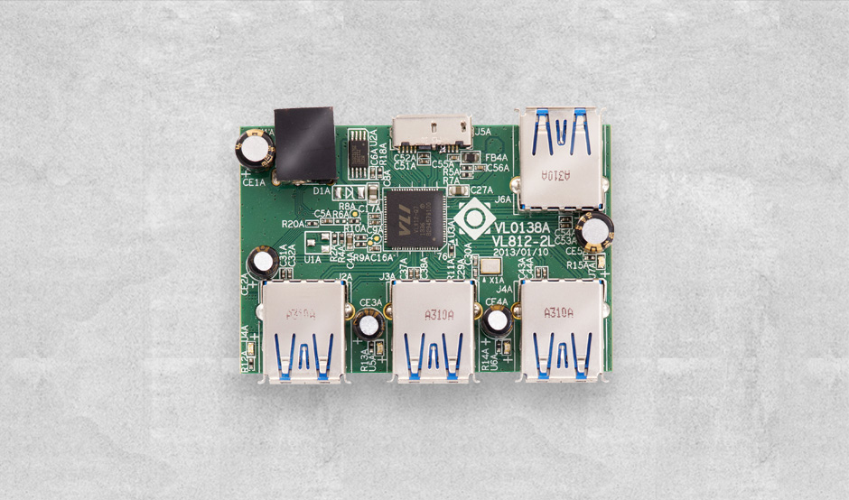
VIA实验室的VL812使四个USB设备可以连接到主机计算机或其他集线器上的单个下游端口。采用先进的CMOS工艺,其集成的内部USB PHY使一个上游端口和四个下游端口支持超高速传输,但也向后兼容以前的USB规格,并提供支持高速(480Mbps),全速度(12Mbps),和低速(1.5Mbps)的流量。VIA实验室内部的USB PHY还具有自适应均衡功能,允许在各种拓扑和信道条件下实现业界领先的信号完整性。
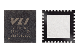
基于VL812的器件采用了精心设计的引脚和先进的制造工艺,可以在最紧凑的器件外壳中享受简单的布局和较低的工作温度。全边带信号引脚可用于显示电源启用,过电流,和LED状态控制。SPI接口支持外部Flash固件升级或额外的软件增强。VIA VL812采用QFN-76L绿色封装(9x9x0.85 mm),适合小尺寸设计。
通过实验室VL812-based中心设备享受完整和全面的驱动支持所有现代操作系统包括Windows、OSX,和Linux,使VL812适合独立的USB集线器,台式电脑前面板中心,车载中心,对接系统,和USB集线器复合设备包括鼠标、键盘、显示器和打印机USB设备。
关键特性
全集成的单片机实现业界领先的集成5V DC-DC交换稳压器。一个上行接口支持超高速、全速度的业务。四个下行接口支持超高速、全速度的业务。 支持USB 3.0低功耗状态。支持全边带信号功能,包括gang模式和LED状态灯。完全软件支持Windows 7, Vista, XP, 2003, 2000, ME和Mac OS 10X以及各种Linux内核
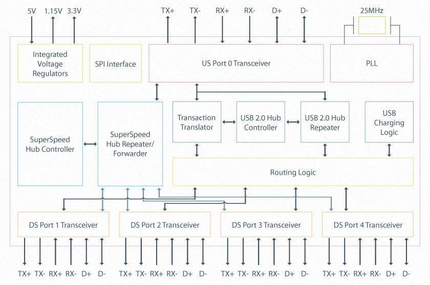
VL812 4-port USB 3.0 hub controller is a 3rd generation fully-integrated single-chip solution which emphasizes low-power design and an industry-first integrated 5V DC-DC switching regulator. VL812 offers high performance, high power efficiency, and reduced overall system BOM, making it an ideal choice for mobile and other low-power applications.
The VIA Lab’s VL812 hub controller supports the higher transfer rates of the USB 3.0 specification, allowing maximum data transfer rates of up to 5Gbps, or ten times the throughput available to USB 2.0. In addition to rapid transfers, VL812 integrates battery charging controller logic, enabling Dedicated Charging Port (DCP) and Charging Downstream Port (CDP) functionality as described in the USB Battery Charging 1.2 specification, as well as a charging in sleep mode feature that supports special vendor modes. When a USB Battery Charging-compatible device is attached, the device can charge over 3 times faster than conventional hubs or hosts. CDP mode allows users to transfer data while simultaneously charging their device at the same rate as when charging from an AC adapter.
The VIA Lab’s VL812 enables four USB devices to be connected to a single downstream port on the host computer or another hub. Employing an advanced CMOS process, its integrated in-house USB PHY enables one upstream port and four downstream ports support Super-Speed transfer, but are also backwards compatible with previous USB specifications and offer support for Hi-Speed (480Mbps), Full-Speed (12Mbps), and Low-Speed (1.5Mbps) traffic. The VIA Labs in-house USB PHY also features adaptive equalization, allowing for industry-leading signal-integrity over a variety of topologies and channel conditions.
Employing a well-planned pin-out and advanced manufacturing process, devices based on VL812 can enjoy easy layout and a low working temperature in the most compact device housing. Full sideband signal pins are available for showing power enable, over current, and LED status control. The SPI interface supports external Flash for firmware upgrades or additional software enhancements. The VIA VL812 is available in a QFN-76L green package (9x9x0.85 mm) to fit small form-factor designs.
VIA Lab’s VL812-based hub devices enjoy full and comprehensive driver support on all modern operating systems including Windows, OSX, and Linux, making the VL812 well suited for stand-alone USB hubs, desktop PC front panel hubs, on-board hubs, docking systems, and USB hub compound devices including mouse, keyboard, display and printer USB devices.
Key Features
Compliant to USB 3.0 specification revision 1.0, and USB specification revision 2.0
Fully integrated single chip implementation
Industry-first integrated 5V DC-DC switching regulator
One up-stream supports Super-speed, high-speed and full-speed traffic
Four down-stream ports support Super-speed, high-speed and full-speed traffic
Charging Downstream Port(CDP), feature for rapid-charging
In-house USB PHY employs advanced CMOS process for low power consumption
Supports USB 3.0 low power states
Supports full sideband signal functions include gang mode and LED status lights
-
Full software support for Windows 7, Vista, XP, 2003, 2000, ME and Mac OS 10X and various Linux kernels
